Probe Boards
Categories:
3 minute read
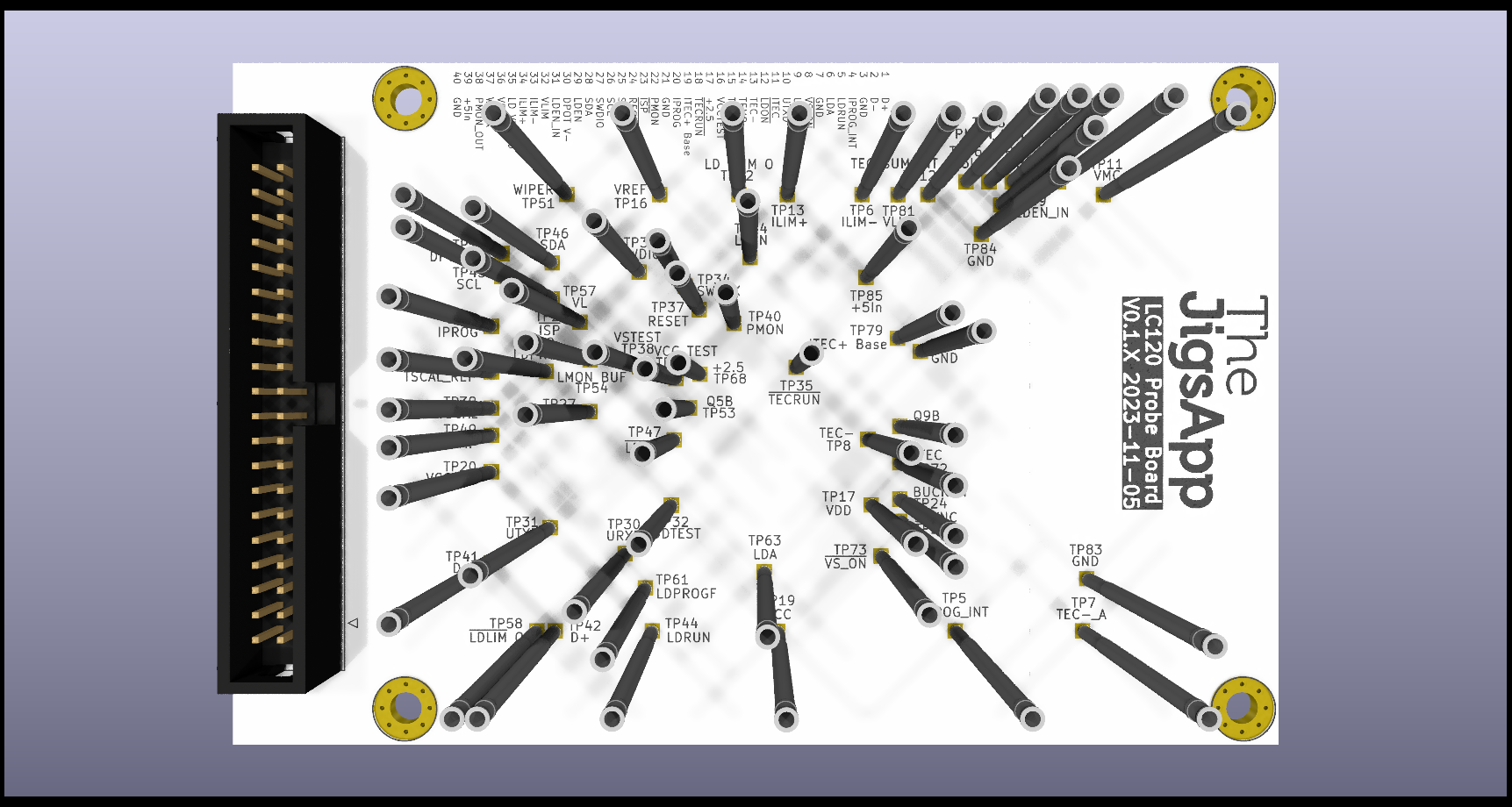
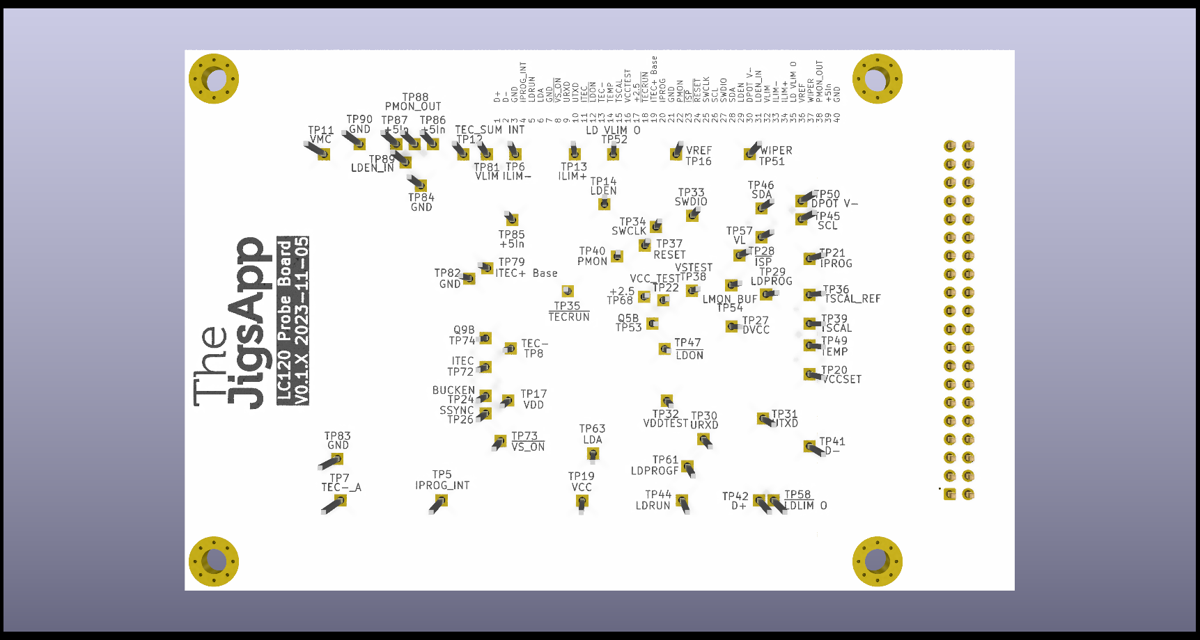
The test probes are electrically connected to your test engine through the probe board. This replaces the time consuming and error prone handwiring method with a PCB. The probe board mounts to the bottom of the cradle and lines up with the test probe sockets which are soldered in place. The probes themselves are removable and replacable whereas the sockets are held in place. This allows your number of test stations to be easily scaled and have the reliability of a PCB instead of individual loose wires.
These boards are available in 2 and 4 layers with 6 layers requiring a special order. Our probe boards are parameterized and auto-generated.
Connectors
Our default connectors are through-hole 2.54mm pin headers, which are good to about 40 MHz. Higher frequency testing is possible as well. Controlling the stray inductance generally requires much shorter pins with less travel, so the most straightforward method is to use a standard jig for most of the functional testing, and a second high-frequency one for the sensitive stuff. Once method of handling that is to do the majority of your functional test with a standard jig and have a second for the high frequency signals.
Auto-generation
Our probe boards are auto-generated using an advanced combinatoric optimizing method wrapped around a traditional autorouter. The routing problem is also far better contrained than a general application so the performance is far better than you’d expect for most auto-routor results. The result is that autogeneration succeeds nearly 100% of the time. We take the specified board and attempt to route it as both a 2 and 4 layer board. Some more complex boards cannot be reliably made using a two-layer board, which will requires using the four-layer. You may want to customize the generated PCB for your specific application, so besides the board Gerbers, we supply the generated PCB as a KiCad project to make that easy.
Two-layer boards are faster and cheaper to source than four-layer. We prefer two-layers when we can make our design without compromising the performance. This isn’t always possible when the specification requires too many traces that cross. One characteristic of test systems is that the connections commonly fall into related classes, which can potentially be interchanged without affecting the function. For instance, there are usually many analog voltages being measured, using a data acquisition brick such as a LabJack. It doesn’t usually matter much which DAQ channel corresponds to which test point, and interchaging these is one of the algorithms used in the auto-generator.
Groups of signals that can be interchanged can be assigned to the connector as a class instead of as a net. Connections assigned to a specific net will not be re-mapped. We will the optimize the layout by changing the net placements within each class to give an optimal layout with fewer layers. We then generate a CSV, JSON, TOML, or YAML configuration file which can be processed by your test software to re-map the assignments.
Dynamic Re-mapping Case Study
- Use Case: Manufacturing EOL
- Signal Groups:
- 16x MUX’d 0-5V analog channels
- SWD
- UART
- USB 2.0
- 2x 0-24V analog outputs
- 5x 5V DIO
In this case we can interchange the signals in group 1, 5, and 6 with other signals in the same group. By using this flexibility to improve the routing we can produce a huge number of designs with only one routing layer and a (nearly) featureless ground plane. The pin mappings are then versioned and can be used for automatically mapping the pins in software.